IEC 60747-9 pdf download
IEC 60747-9 pdf download.Semiconductor devices – Discrete devices
1 Scope
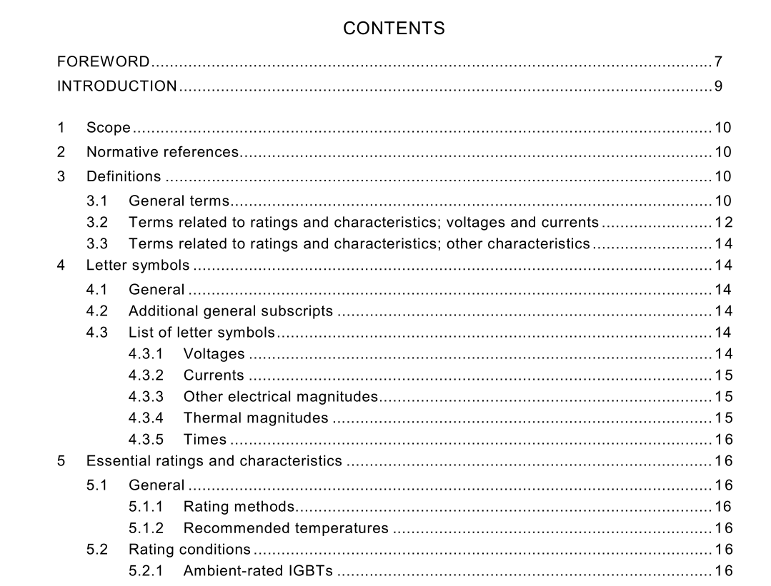
This part of IEC 60747 gives product specific standards for terminology, letter symbols, essential ratings and characteristics and measuring methods for insulated-gate bipolar transistors (IGBTs).
2 Normative references
The following normative documents contain provisions which, through reference in this text, constitute provisions of this part of IEC 60747. At the time of publication, the editions indicated were valid. All normative documents are subject to revision, and parties to agreements based on this part of IEC 60747 are encouraged to investigate the possibility of applying the most recent editions of the normative documents indicated below. Members of IEC and ISO maintain registers of currently valid International Standards. IEC 60617-5:1996, Graphical symbols for diagrams – Part 5: Semiconductors and electron tubes IEC 60747-1:1983, Semiconductor devices – Discrete devices and integrated circuits – Part 1: General IEC 60747-2:1983, Semiconductor devices – Discrete devices and integrated circuits – Part 2: Rectifier diodes IEC 60747-7:2000, Semiconductor discrete devices and integrated circuits – Part 7: Bipolar transistors
3 Definitions
For the purpose of this standard, the following definitions apply. 3.1 General terms 3.1.1 insulated-gate bipolar transistor (IGBT) transistor provided for power switching having a conduction channel and a PN junction and in which the current flowing through the channel and the junction is controlled by an electric field resulting from a voltage applied between the gate and emitter terminals NOTE With collector-emitter voltage applied the PN junction is forward biased. 3.1.2 N-channel IGBT IGBT that has one or more N-type conduction channels 3.1.3 P-channel IGBT IGBT that has one or more P-type conduction channels 3.1.4 collector current (I c ) (of an IGBT) direct current that is switched (controlled) by the IGBT 3.1.5 collector terminal, collector (C) (of an IGBT) for an N-channel (a P-channel) IGBT the terminal to (from) which the collector current flows from (to) the external circuit 3.1.6 emitter terminal, emitter (E) (of an IGBT) for an N-channel (a P-channel) IGBT the terminal from (to) which the collector current flows to (from) the external circuit 3.1.7 gate terminal, gate (G) (of an IGBT) terminal to which a voltage is applied against the emitter terminal in order to control the collector current 3.2 Terms related to ratings and characteristics; voltages and currents 3.2.1 collector (-emitter) breakdown voltage (V (BR)CES ) voltage between collector and emitter above which the collector current rises steeply, with gate to emitter short-circuited 3.2.2 collector (-emitter) saturation voltage (V CEsat ) collector-emitter voltage under conditions of gate-emitter voltage at which the collector current is essentially independent of the gate-emitter voltage 3.2.3 (gate-emitter) threshold voltage (V GE(TO) ) gate-emitter voltage at which the collector current has a specified low (absolute) value 3.2.4 collector (-emitter) cut-off current (I CES ) collector current at a specified collector-emitter voltage below the breakdown region and with gate to emitter short-circuited 3.2.5 gate leakage current (I GES ) leakage current into the gate terminal at a specified gate-emitter voltage with the collector terminal short-circuited to the emitter terminal3.2.6 tail current (I CZ ) collector current during the tail time 3.2.7 collector(-emitter) voltage with gate-emitter short-circuited (V CES ) collector-emitter voltage at which the collector current has a specified low (absolute) value with gate-emitter short-circuited 3.2.8 collector-emitter sustaining voltage (V CE*sus ) collector-emitter breakdown voltage at relatively high values of collector current where the breakdown voltage is relatively insensitive to changes in collector current, for a specified termination between gate and emitter terminals NOTE 1 The specified termination between gate and emitter terminals is indicated in the letter symbol by the third subscript ‘*’; see 4.1.2 of IEC 60747-7. NOTE 2 When necessary, a suitable qualifier is added to the basic term to indicate a specific termination between gate and emitter terminals. Example: Collector-emitter sustaining voltage with gate and emitter terminals short-circuited V CESsus . NOTE 3 The basic term may be shortened if the meaning is clear from the letter symbol used. Example: Collector-emitter sustaining voltage V CERsus . NOTE 4 This term is important for high-voltage devices, for example more than 4 kV. 3.2.9 electrostatic discharge voltage Under consideration. 3.3 Terms related to ratings and characteristics; other characteristics 3.3.1 input capacitance (C ies ) capacitance between the gate and emitter terminals with the collector terminal short-circuited to the emitter terminal for a.c 3.3.2 output capacitance (C oes ) capacitance between the collector and emitter terminals with the gate terminal short-circuited to the emitter terminal for a.c
